TASC has mastered silicon-based and compound semiconductor epitaxy technology. We also offer professional design and chip fabrication. These are combined with robust quality control to create world-class sensing components, including a variety of photo-sensing component solutions.
such as photodiodes, phototransistors, photo-sensing controllable thyristors, and Zener diodes used in everyday applications such as wearable health management, industrial, automotive, and home appliance products.

Mechanism

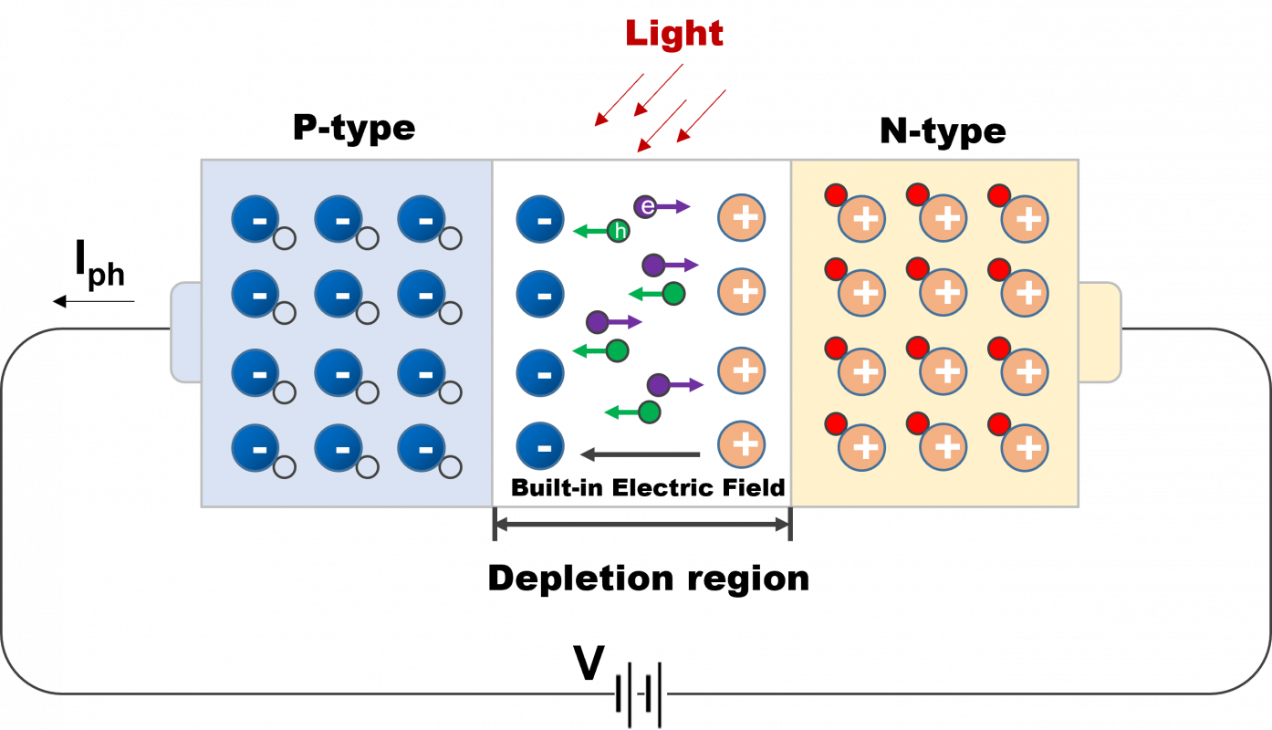
When an equipped with enough energy photon hit the photodiode and the absorption occurs in the depletion region, the built-in electric field will make the electron-hole pair move toward the anode and the cathode to generate the photo current. In fact, the light signal is the sum of the photo current and dark current. Thus, the dark current regarded as a noise should be effectively reduced to increase the sensitivity on the device.
Device Structure

The photodiode is composed of PN junction. Inserting the intrinsic layer with high resistivity will form the PIN structure which increase the effective width of depletion layer. Apart from increasing the breakdown voltage, it also generates large amount of electron-hole pair to increase quantum efficiency. Moreover, it further reduces the junction capacitance to raise device switching speed.

Material selection

Because the photodiode is sensitive to particular wavelength range, so according to wavelength of light source, the corresponding materials will be chosen to do detection. The materials shown below :

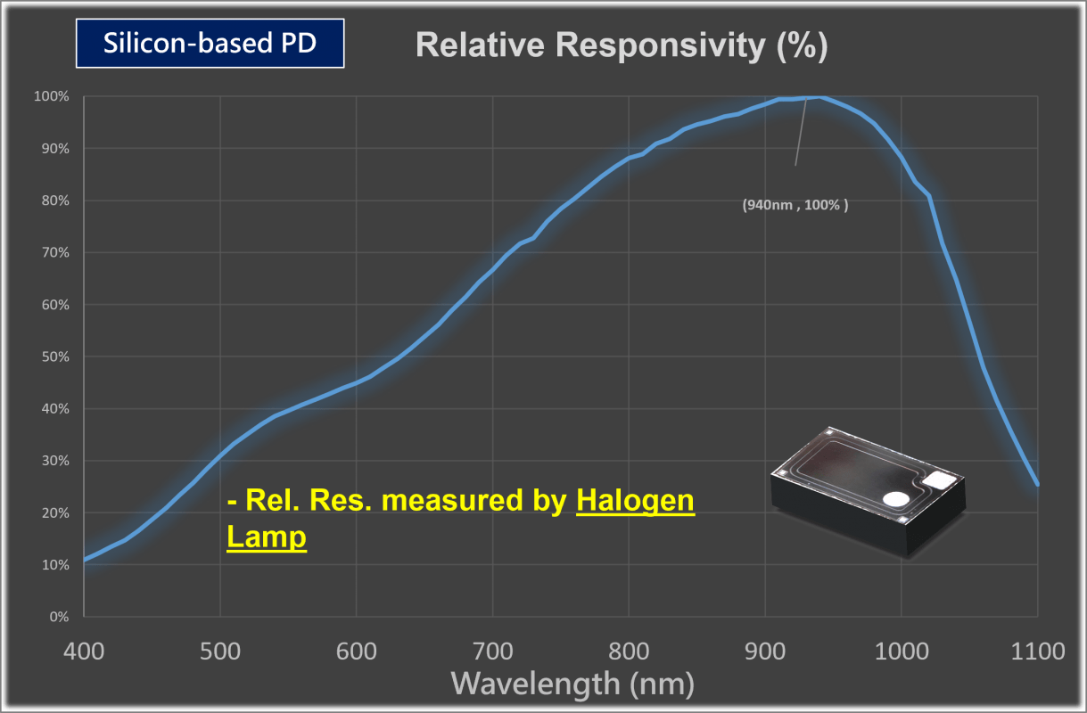
Silicon-based PD : Common sensing wavelength within 400~1100 nm
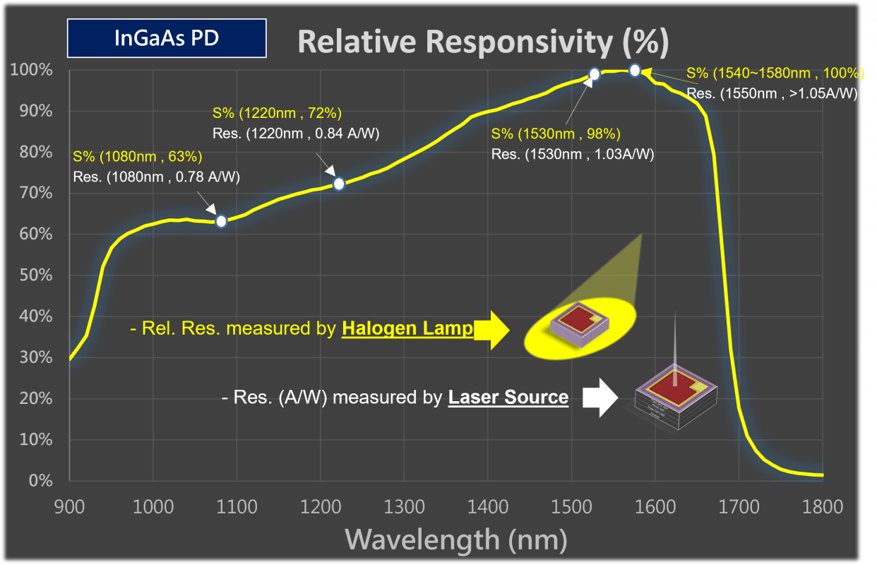
Compound PD : InGaAs PD, common sensing wavelength within 900~1700nm

Characteristics

Responsivity : The conversion efficiency between radiant optical power and the generated current ; The unit is Ampere/Watt (A/W), which can also be converted to quantum efficiency (%)
Dark current : The internal flowing current in the optical sensing device with no incident light environment ; The unit is nA
Breakdown Voltage : The minimum reverse bias voltage when diode reverse conducting
Responsivity spectrum : The line diagram of photocurrent conversion efficiency over different wavelength of incident light source. The light spectral shown as below :
Mechanism

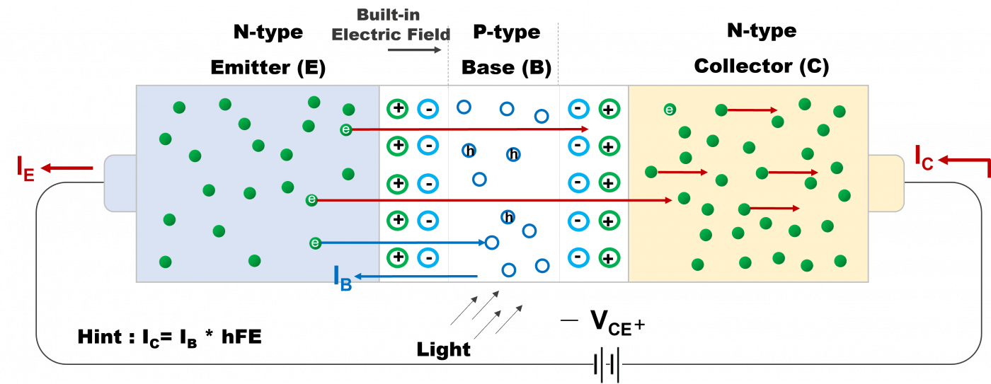
The phototransistor is a kind of NPN junction device which is similar to photodiode. When illumination, the photon will impact the base and act as a applied voltage to base (VBE). The emitter electron current flows to base and recombine with holes to generate the small current (IB) which is proportional to illumination of incident light. Besides, because the base thickness is generally thin, so the electron that flows from emitter to the base will diffuse to collector and is attracted by the forward voltage between collector-emitter. Therefore, the generated collector current (IC) will be amplified according to the current gain (hFE) of the phototransistor.

Device Type

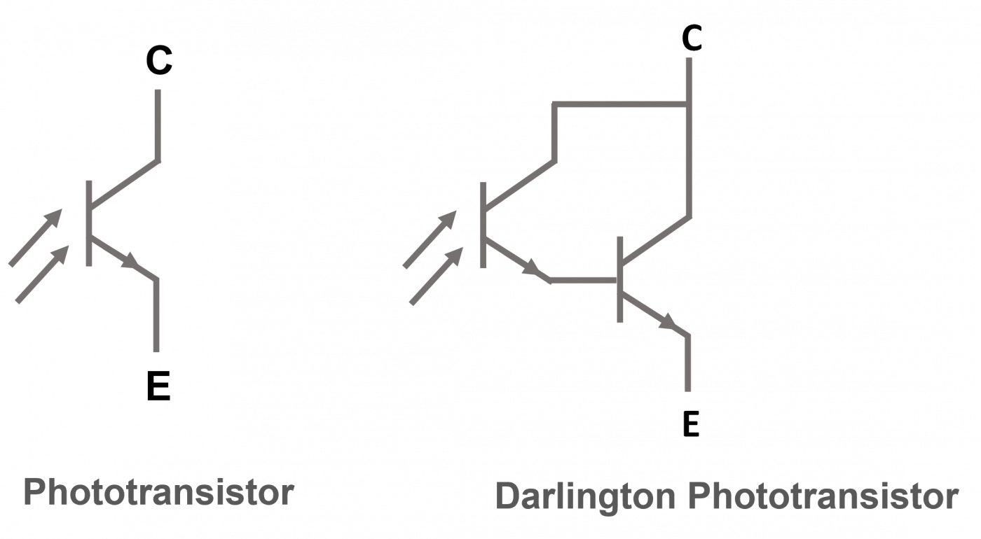
Phototransistor is mainly composed of NPN junction or two phototransistors form Darlington phototransistor in order to acquire the larger gain (hFE)

Characteristics

BVCEO : The minimum voltage makes collector-emitter junction collapse when base is open circuit
BVECO : The minimum voltage makes emitter-collector junction collapse when base is open circuit
ICEO : The leakage current flowing to collector-emitter when base is open circuit with no illumination
VCE(S) : The maximum voltage of collector-emitter makes the PN junction forward biasing
hFE : The amplified current gain between collector current and the generated photo current in the base

The phototransistor in photocoupler

1. It contains the light emitted, light received and signal amplified to accomplish the electric-light-electric conversion
2. The input the output completely achieve the electrical isolation with one-way transmission and the output signal has no influence on input
3. The current transfer ratio is defined as the ratio of output current (IC) to input current (IF). It mainly estimates the load resistance (RL) selection
4. Commonly apply to signal isolation switch and signal transmission

Mechanism

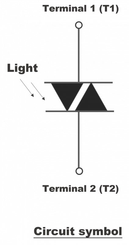
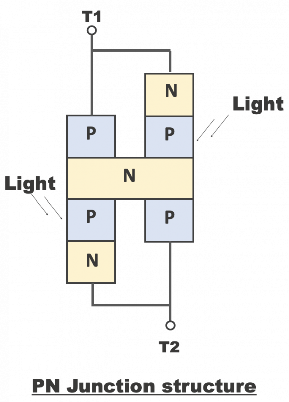
The phototriac is regarded as a pair of PNPN junction (Similar to Darlington phototransistor operation) in reverse parallel connection with two electrodes of T1 and T2. When the control gate is triggered after light illumination, it will make the phototriac conducted no matter what the polarity voltage applied to the T1 & T2.

Operation Type

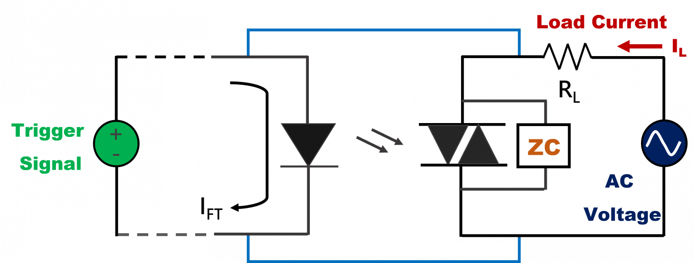
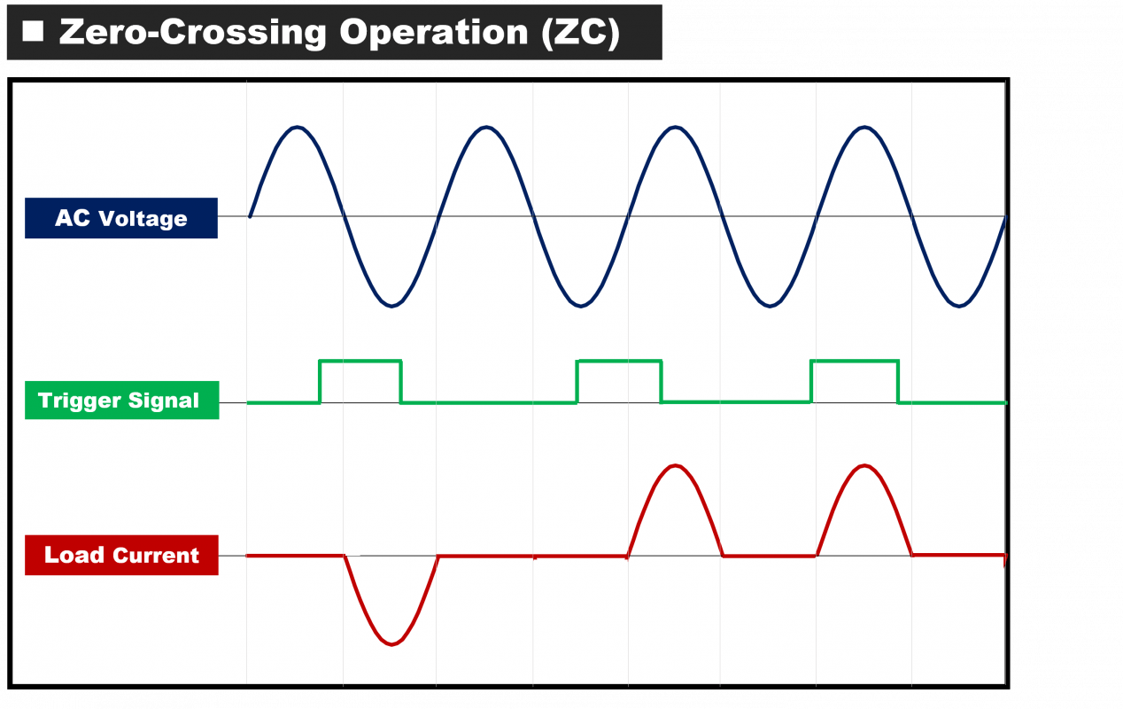
1. Zero-Crossing (ZC):

For 60Hz AC power supply, there are sixty sine wave cycles and sixty crossing points to zero voltage. When turning on or switching off at this moment, it doesn’t quite occur the sparkle in order to extend the life of switch connection node.
If using the light triggering thyristor with much shorter conducting time characteristics as a control switch which drives external connection node at the zero crossing, it is able to surpass those of longer reaction time in conventional
electromagnetic relay which is unable to reach in the zero-cross switching

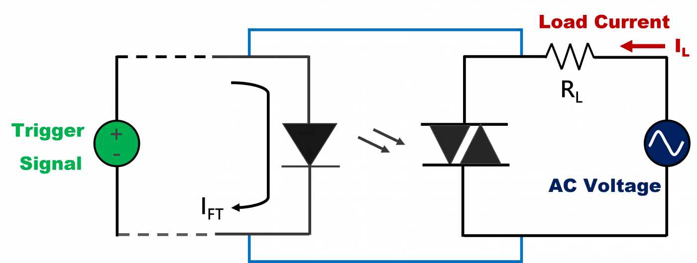
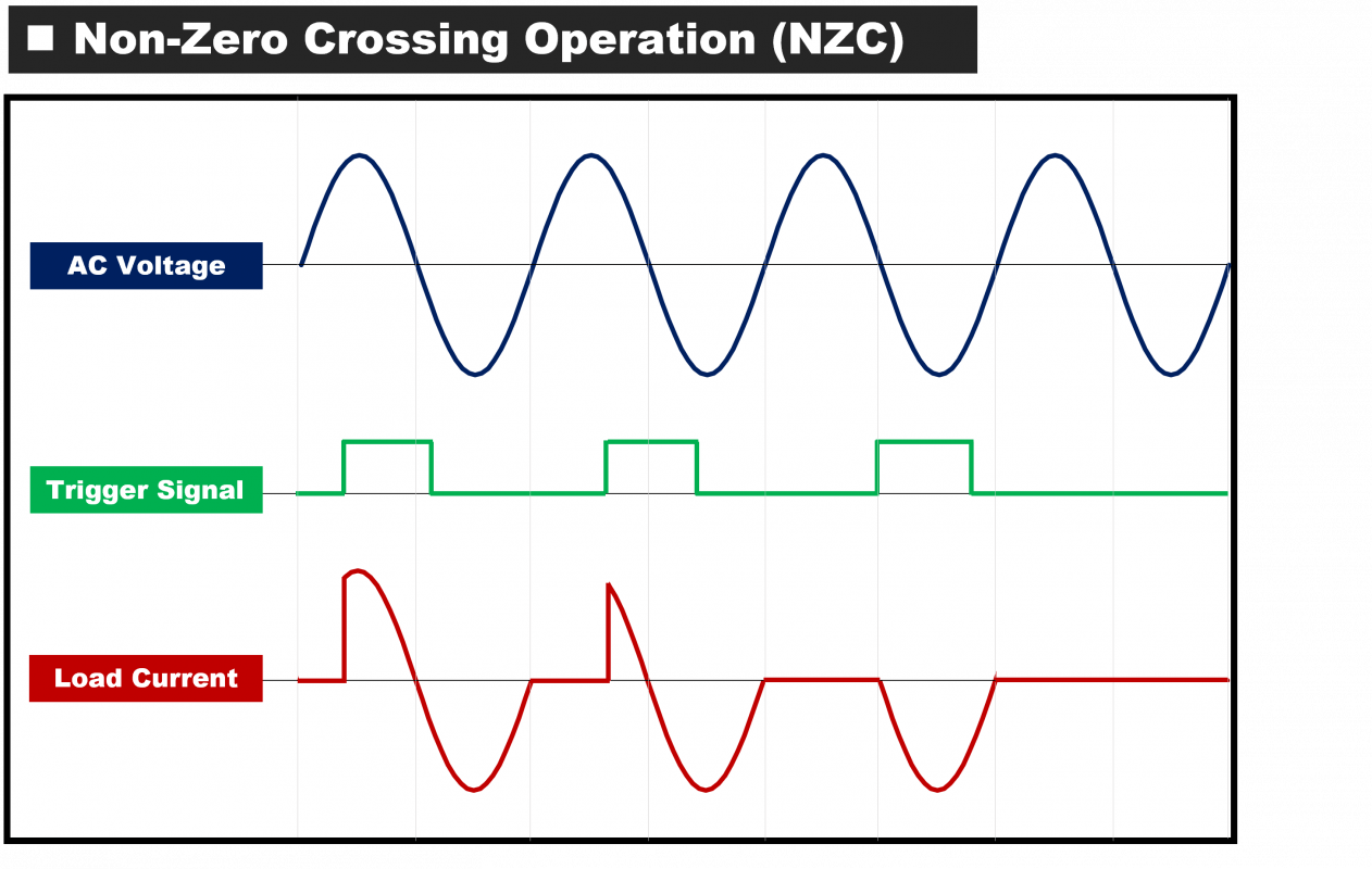
2. Non-zero crossing (NZC):

What differs from ZC is that the NZC allows to output voltage at any time of AC sine wave. Therefore, because the output voltage wave form is not always the competed sine wave so it can control the phase angle to output different power

Key Characteristics

Repetitive peak off-state voltage (VDRM) : A forward peak voltage that can be repetitively applied to the terminals in the conditions of control-gate open and phototriac forward blocking
Peak on-state voltage : The peak voltage across the device while it is on-state
dV/dt : The maximum value of rate of the rising voltage that can be applied across the terminals of the phototriac
Holding current (IH) : The minimum current level continues to keep the device conducting in the conditions of the specified environment temperature and no control gate current is applied
Inhibit Voltage (VINH) : When loading voltage is higher than inhibit voltage in the ZC circuit, it can prevent phototriac from triggering even though the trigger current is high